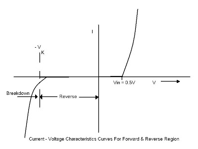
A p-n junction is a two-terminal device that acts as a one-way conductor. When a diode is forward biased as shown in Figure1 (a), Current flows through the diode and current is given by
ID = IS (e Vo/nVT – 1) ------ (1)
When, n is the ideality factor and 1 ≥ n ≥ 2. IS is the reverse-saturation current and VT = KT/ q is the thermal voltage. VT is about 0.026V at room temperature.
When it is reverse biased as shown in Figure, ID = - IS. As it is generally in PA (Pico-Amp) range, in many applications this current is neglected and diode is considered open
ID = IS (e –VR/VT - 1) = - IS for | V | >> VT ------- (2)
The material for p-n junction diode is silicon semiconductor. Semiconductors are a group of materials having electrical conductivity intermediate between metals and insulators. Metals: Al (Aluminum), Cu (Copper), Au (gold), Insulators: Ceramic, Wood, Rubber. Semiconductor: Si (Silicon), Ge (Germanium), GaAs (Gallium-Arsenide).
Apparatuses: -
· p-n junction diode (1N4003) ---- 1 Piece
· 5V Zener Diode ------------------- 1 Piece
· Resistor (1K) ---------------------- 1 Piece
· DC Power Supply ---------------- 1 Piece
· Signal Generator ----------------- 1 Piece
· Oscilloscope ---------------------- 1 Piece
· Chords and Wire ----------------- Lot
| VS (Volt) | VR Ω | VD (Volt) | ID (mA) |
| 0.1 | 0 | 0.16 | 0 |
| 0.5 | 0.12 | 0.46 | 0.12 |
| 0.7 | 0.24 | 0.5 | 0.24 |
| 1.0 | 0.5 | 0.53 | 0.5 |
| 1.5 | 1.0 | 0.36 | 1.0 |
| 2.0 | 1.5 | 0.6 | 1.5 |
| 2.5 | 2.0 | 0.6 | 2.0 |
| 3.0 | 2.5 | 0.61 | 2.5 |
| 3.5 | 3.0 | 0.62 | 3.0 |
| 4.0 | 3.5 | 0.63 | 3.5 |
| 4.5 | 4.0 | 0.63 | 4.0 |
| 5.0 | 4.5 | 0.63 | 4.5 |
Data Table of Reverse Region: -
| (Volt) | VR Ω | VD (Volt) | ID (mA) |
| 0.1 | 0 | 0.15 | 0 |
| 0.3 | 0 | 0.34 | 0 |
| 0.5 | 0 | 0.54 | 0 |
| 0.7 | 0 | 0.72 | 0 |
| 1.0 | 0 | 1.03 | 0 |
| 2.0 | 0 | 2.05 | 0 |
| 3.0 | 0 | 3.11 | 0 |
| 4.0 | 0 | 4.06 | 0 |
| 5.0 | 0.04 | 5.05 | 0.04 |
| 6.0 | 0.52 | 5.56 | 0.52 |

Procedure: -
- Measure resistance accurately using multimeter. Construct the circuit as shown in Figure- 2. Vary input voltage (Vdc) and measure VD, VR for values of VD = 0.1V, 0.2V, 0.3V, 0.4V, 0.5V, 0.6V, 0.7V and so on. Obtain maximum value of VD without increasing Vdc beyond 25V (Note that ID = VR/R).
- Repeat step-1 for the values at VZ = 0.5V, 1.0V, 1.5V, 2.0V, 2.5V, 3.0V and so on up to the maximum value obtainable without increasing Vdc beyond 25V. Apply circuit in Figure-3 for this step.
- Construct the circuit as shown in the Figure-4. Set the oscilloscope in X-Y mode and locate the zero point on oscilloscope display. Make proper connection (according to Figure-4) and observe the output.
- Repeat step-3 by increasing supply frequency to 5 KHz.
Report: -
- Plot diode I-V chrematistics for different reading obtained in this experiment.
- Explain the result obtained in Figure-1, 2, 3, 4.

No comments:
Post a Comment