Tuesday, February 17, 2009

Experiment: Study of Diode Rectifier Circuits

Theory: -
The diode rectifier converts the input sinusoidal voltage Vs to a unipolar out Vo. There are two types of rectifier circuits:
  1. Half-wave Rectifier and
  2. Full-wave Rectifier.
Apertures: -

1. Trainer Board
2. Multimeter
3. Resistor 10KΩ
4. Capacitor 1μF, 47μF
5. Diode Four Pieces
6. Oscilloscope
7. Signal Generator
8. Wire.

Circuit Diagram For Half-wave Rectifier:


The input and output of the rectifier are drawn in Figere-1. Diode conducts only when it is forward biased. For Vs = Vm sinωt, DC voltage and current of a half-wave rectifier are as follows

VDC = Vm/π – (1/2)VDO

IDC = {Vm/π – (1/2)VDO}/R

Where VDO ≈ 0.7 V

PIV (Peak Inverse Voltage): -

PIV is the Peak Reverse Voltage that appears across the diode when it is reverse-biased,

PIV = Vm

Circuit Diagram For Full-wave Rectifier: -


The bridge rectifier circuit and their input and output voltage as a function of time is shown below. Peak voltage across each diode when it is reverse-biased

PIV = Vm – VDO

DC Voltage, VDC = 2Vm/π – 2 VDO

Ripple Factor: -

A rectifier converting alternating currents into a unidirectional current, periodically fluctuating components still remaining in the output wave. A measure of the fluctuating component is given by the ripple factor r, which is defined as

R = rms value of alternating components of wave/Average value of wave

= I’ rms/Idc = V’ rms/Vdc

Where, I’ rms and V’ rms denote the rms value of the ac components of the current and voltage, respectively.

For a half-wave rectifier, r = 1.21 and for a full wave rectifier, r = 0.482

Calculating Ripple Factor for Half-wave Rectifier: -

For C = 1μF,

The DC value is 0.5V

The rms value is 0.5V

So the Ripple Factor is 0.5/0.5 = 1

For C = 47μF,

The DC value is 5V

The rms value is 0.9V

So the Ripple Factor is 0.9/5 = 0.18

Calculating Ripple Factor for Full-wave Rectifier: -

For C = 1μF,

The DC value is 0.9V

The rms value is 0.22V

So the Ripple Factor is 0.22/0.9 = 0.24

For C = 47μF,

The DC value is 8.78V

The rms value is 6.18V

So the Ripple Factor is 6.18 /8.78 = 0.7

Procedure: -

1. Construct circuit of Figure-1 without the capacitor. Observe Vi and Vo simultaneously on the oscilloscope. Sketch input and output waveforms. Measures Vo with multimeter in dc and ac mode.

2. Connect 1μF capacitor across the load resistor. BE CAREFUL about the polarity of the capacitor. Sketch input and output waveforms. Measure Vo with multimeter.

3. Replace 1μF capacitor with 47μF and repeat step-2.

4. Construct the circuit of Figure-2 without the capacitor. Observe and sketch Vi, Vo. DO NOT TRY to observe Vi, Vo simultaneously. Measure AC and DC components of Vo with multimeter.

5. Connect 1μF capacitor as shown in Figure-2 and repeat step-4.

6. Replace 1μF capacitor by 47μF for Figure-2 and repeat step-4.


Experiment: Study of Diode Characteristics

Theory: -
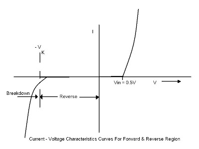
A p-n junction is a two-terminal device that acts as a one-way conductor. When a diode is forward biased as shown in Figure1 (a), Current flows through the diode and current is given by

ID = IS (e Vo/nVT – 1) ------ (1)

When, n is the ideality factor and 1 ≥ n ≥ 2. IS is the reverse-saturation current and VT = KT/ q is the thermal voltage. VT is about 0.026V at room temperature.

When it is reverse biased as shown in Figure, ID = - IS. As it is generally in PA (Pico-Amp) range, in many applications this current is neglected and diode is considered open

ID = IS (e –VR/VT - 1) = - IS for | V | >> VT ------- (2)

The material for p-n junction diode is silicon semiconductor. Semiconductors are a group of materials having electrical conductivity intermediate between metals and insulators. Metals: Al (Aluminum), Cu (Copper), Au (gold), Insulators: Ceramic, Wood, Rubber. Semiconductor: Si (Silicon), Ge (Germanium), GaAs (Gallium-Arsenide).

Apparatuses: -

· p-n junction diode (1N4003) ---- 1 Piece

· 5V Zener Diode ------------------- 1 Piece

· Resistor (1K) ---------------------- 1 Piece

· DC Power Supply ---------------- 1 Piece

· Signal Generator ----------------- 1 Piece

· Oscilloscope ---------------------- 1 Piece

· Chords and Wire ----------------- Lot

Data Table of Forward Region: -

VS (Volt)

VR

VD (Volt)

ID (mA)

0.1

0

0.16

0

0.5

0.12

0.46

0.12

0.7

0.24

0.5

0.24

1.0

0.5

0.53

0.5

1.5

1.0

0.36

1.0

2.0

1.5

0.6

1.5

2.5

2.0

0.6

2.0

3.0

2.5

0.61

2.5

3.5

3.0

0.62

3.0

4.0

3.5

0.63

3.5

4.5

4.0

0.63

4.0

5.0

4.5

0.63

4.5

Data Table of Reverse Region: -

(Volt)

VR

VD (Volt)

ID (mA)

0.1

0

0.15

0

0.3

0

0.34

0

0.5

0

0.54

0

0.7

0

0.72

0

1.0

0

1.03

0

2.0

0

2.05

0

3.0

0

3.11

0

4.0

0

4.06

0

5.0

0.04

5.05

0.04

6.0

0.52

5.56

0.52


Procedure: -
  1. Measure resistance accurately using multimeter. Construct the circuit as shown in Figure- 2. Vary input voltage (Vdc) and measure VD, VR for values of VD = 0.1V, 0.2V, 0.3V, 0.4V, 0.5V, 0.6V, 0.7V and so on. Obtain maximum value of VD without increasing Vdc beyond 25V (Note that ID = VR/R).
  2. Repeat step-1 for the values at VZ = 0.5V, 1.0V, 1.5V, 2.0V, 2.5V, 3.0V and so on up to the maximum value obtainable without increasing Vdc beyond 25V. Apply circuit in Figure-3 for this step.
  3. Construct the circuit as shown in the Figure-4. Set the oscilloscope in X-Y mode and locate the zero point on oscilloscope display. Make proper connection (according to Figure-4) and observe the output.
  4. Repeat step-3 by increasing supply frequency to 5 KHz.


Report: -

  1. Plot diode I-V chrematistics for different reading obtained in this experiment.
  2. Explain the result obtained in Figure-1, 2, 3, 4.